CY2PP326
CY2PP326 is 2 x 2 Clock and Data Switch Buffer manufactured by Cypress.
Features
- Six ECL/PECL differential outputs
- Two ECL/PECL differential inputs
- Hot-swappable/-insertable
- 50 ps output-to-output skew
- 250 ps device-to-device skew
- 950 ps propagation delay (typical)
- 1.2 GHz Operation
- 2.8 ps RMS period jitter (max.)
- PECL mode supply range: VEE =
- 2.5V± 5% to
- 3.3V±5% with VEE = 0V
- ECL mode supply range: VCC = 2.5V± 5% to 3.3V±5% with VEE = 0V
- Industrial temperature range:
- 40°C to 85°C
- 32-pin 1.4mm TQFP package
- Temperature pensation like 100K ECL
- Pin patible with MC100ES6254
Functional Description
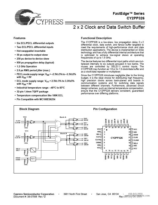
The CY2PP326 is a low-skew, low propagation delay 2 x 2 differential clock, data switch, and fanout buffer targeted to meet the requirements of high-performance clock and data distribution applications. The device is implemented on Si Ge technology and has a fully differential internal architecture that is optimized to achieve low-signal skews at operating frequencies of up to 1.5 GHz. The device features two differential input paths which are multiplexed internally to six outputs grouped in two banks. The muxes are controlled by SEL(0:1) control inputs. The CY2PP326 may function as 1:6 or 2x 1:3 clock/data buffer and as a clock/data repeater or multiplexer. Since the CY2PP326 introduces negligible jitter to the timing budget, it is the ideal choice for distributing high frequency, high precision clocks across back-planes and boards in munication systems and for switching data signals between different channels. Furthermore, advanced circuit design schemes, such as internal temperature pensation, ensure that the CY2PP326 delivers consistent, guaranteed performance over differing platforms.
Block Diagram
VCC CLK0 CLK0# VEE VCC
0 1
Pin Configuration
Bank A
QA0#
QA1#
QA2#
QA0
QA1
QA1 QA1# QA2 QA2#
VCC VEE SEL1 CLK1 CLK1# OEB# VEE VCC
1 2 3 4 5 6 7 8
32 31 30 29 28 27 26 25 24 23 22
QA2
QA0 QA0#
VCC VEE OEA# CLK0 CLK0# SEL0 VEE VCC
B ank...